
Let’s continue to learn the the process about creating bumps.
1. Wafer Incoming and Clean:
Before starting the process, the wafer surface may have organic contaminants, particles, oxide layers, etc., which need to be cleaned, either by wet or dry cleaning methods.
2. PI-1 Litho: (First Layer Photolithography: Polyimide Coating Photolithography)
Polyimide (PI) is an insulating material that serves as insulation and support. It is first coated on the wafer surface, then exposed, developed, and finally the opening position for the bump is created.
3. Ti / Cu Sputtering (UBM):
UBM stands for Under Bump Metallization, which is mainly for conductive purposes and prepares for subsequent electroplating. UBM is typically made using magnetron sputtering, with the seed layer of Ti/Cu being the most common.
4. PR-1 Litho (Second Layer Photolithography: Photoresist Photolithography):
The photolithography of the photoresist will determine the shape and size of the bumps, and this step opens the area to be electroplated.
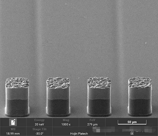
5. Sn-Ag Plating:
Using electroplating technology, tin-silver alloy (Sn-Ag) is deposited at the opening position to form bumps. At this point, the bumps are not spherical and have not undergone reflow, as shown in the cover image.
6. PR Strip:
After electroplating is completed, the remaining photoresist (PR) is removed, exposing the previously covered metal seed layer.
7. UBM Etching:
Remove the UBM metal layer (Ti/Cu) except in the bump area, leaving only the metal under the bumps.
8. Reflow:
Pass through reflow soldering to melt the tin-silver alloy layer and allow it to flow again, forming a smooth solder ball shape.
9. Chip Placement:
After the reflow soldering is completed and the bumps are formed, the chip placement is carried out.
With this, the flip chip process is complete.
In the next new, we will learn the process about chip placement.


