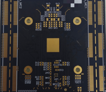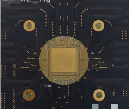

Science and technology are increasingly advancing, and people's level of observation of things is getting deeper and deeper. The product we bring today is an optical chip substrate used on single-photon avalanche diode (SPAD) imaging detectors. Single-photon avalanche diodes (SPADs) play an important role in many fields, including but not limited to astronomy, flow cytometry, fluorescence lifetime imaging microscopy (FLIM), particle sizing, quantum computing, quantum key distribution, and single-molecule detection.
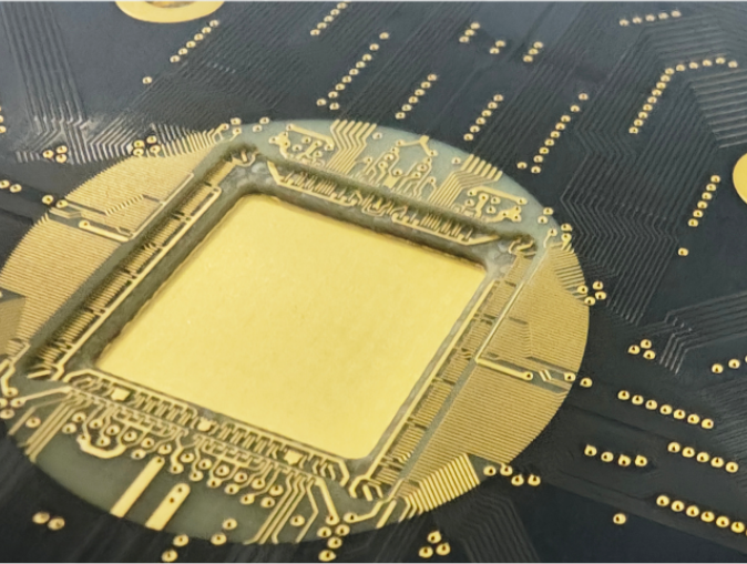
The most challenging part of the product's process is the two-step staircase in the picture on the top, which requires two controlled-depth routings and laser opening. The requirements for controlling the depth are very strict.
| The surface treatment used is a nickel palladium gold process. The nickel palladium gold surface treatment has strong adhesion, is not easy to fall off, and enhances the product's reliability and stability. |  |
 |
The surface treatment used is a nickel palladium gold process. The nickel palladium gold surface treatment has strong adhesion, is not easy to detach, and enhances the product's reliability and stability. Additionally, as a substrate, the product's circuit design is of high precision and highly integrated. The design of line width and spacing is only 2mil. The smallest bonding pad is 0.070mm. |
IC Carrier PCB are specialized printed circuit boards designed to carry electronic components, characterized by high precision, high reliability, and high integration. They possess excellent electrical, mechanical, and thermal properties, meeting the high-performance demands of various complex electronic systems. The process flow may not be as complex as imagined, but the parameters at the detail level are very strict.
If you want to take a PCB like this OC PCB, just click the button on the top to contact us for ordering.