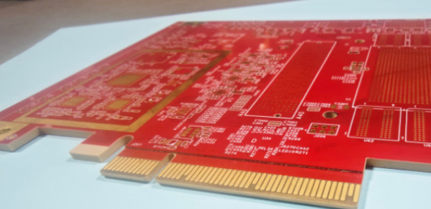

Bright red solder mask ink, gold plating + gold-finger surface treatment process of 30U', makes the entire product appear very high-end. However, what truly attracts people to this product is not just its appearance, but its complex design and precise manufacturing process.
Firstly, let me introduce you to its multilayer construction.
The conventional multi-layer process involves using non-flowable PP (polyimide) film to press and laminate the steps. However, our product requires high-speed performance, so the entire board uses Panasonic's M6 series high-speed PCB substrate. Currently, there is no corresponding non-flowable PP available on the market for M6, so we have to use flowable PP for lamination, which poses a significant challenge for the production of the step sections.
The product is also an 18-layer mechanical blind-hole board.
The product's motherboard is divided into two sub-boards, L1-4 and L5-18, for manufacturing, and the final product is made through three lamination processes. Laminating multi-layer boards is inherently challenging, and when it comes to multi-layer special material boards, even the slightest error during lamination can result in a complete waste of effort!
Finally, to ensure high-speed signal transmission, reduce signal attenuation, ensure stronger and more reliable signals, and also to prevent signal distortion issues, we have also incorporated back drilling technology in the product manufacturing process.
CKT-1 drills from the top layer to the bottom layer with a depth of 1.25+1-0.05, CKB-1 drills from the bottom layer to the top layer with a depth of 0.35mm 1.45+/-0.05, 0.351mm depth 1.25+1-0.05, 0.352mm depth 1.05+/-0.05, 0.353mm depth 0.2+1-0.05.
If you want to take a PCB like this FPGA PCB, just click the button on the top to contact us for ordering.