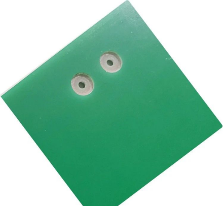

Let’s continue to learn about the various types of holes found on HDI PCB.
1. Blind Via
Blind via, also known as blind holes, are holes that are visible from one surface of the PCB but not from the other. They connect the internal layers to the external layers of the PCB without penetrating through all layers. Blind via function on one side of the board and are used to connect specific layers for signal transmission. They can reduce the complexity of routing on the board, improve signal integrity, and save space. Blind via are commonly used in high-density interconnect and multi-layer PCB designs, such as in smartphones and tablet computers. Blind via are typically laser-drilled holes.
2. Buried Via
Buried via are located within the PCB and do not connect to its surface. They are typically used as power or ground connections to provide better electrical performance and resistance to interference. Buried via can reduce the thickness, weight, and size of the PCB and can optimize signal transmission paths in high-density designs. Generally, buried via use mechanical drilling, but in the industry of any-layer design, laser drilling is also commonly used.
3. Sunk hole
Sunk hole, also known as counterbored holes, flat head holes, or stepped holes, are designed to recess the head of a screw below the surface, with the larger hole accommodating the screw head and the smaller hole for inserting the bolt to secure it in place. These types of holes are commonly used in mechanical manufacturing and construction fields to ensure a flush surface and are typically created using mechanical drilling or laser cutting processes .
More kinds of holes will be shown in the next new.