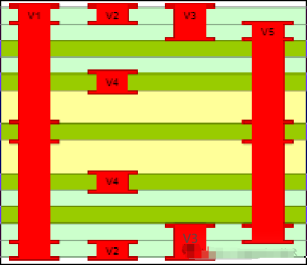

Next, we continue to study the electroplating capabilities of high aspect ratio HDI boards.
I. Product Information:
- Board thickness: 2.6mm, minimum through-hole diameter: 0.25mm,
- Maximum through-hole aspect ratio: 10.4:1;
II. Blind Vias:
- 1) Dielectric thickness: 70um (1080pp), hole diameter: 0.1mm
- 2) Dielectric thickness: 140um (2*1080pp), hole diameter: 0.2mm
III. Parameter Setting Schemes:
Scheme One: Direct electroplating after copper plating
- Using a high acid low copper solution ratio, along with H electroplating additives; current density 10ASF, electroplating time 180min.
-- Final continuity test results
This batch of products had a 100% open circuit defect rate in the final continuity test, with a 70% open circuit defect rate at the 0.2mm blind via location (PP is 1080*2).
Scheme Two: Using conventional electroplating solution to plate the blind vias before plating the through-holes:
1) Using VCP to plate the blind vias, with a conventional acid copper ratio and H electroplating additives, electroplating parameters 15ASF, electroplating time 30min
2) Using a gantry line to thicken, with a high acid low copper ratio and H electroplating additives, electroplating parameters 10ASF, electroplating time 150min
-- Final continuity test results
This batch of products had a 45% open circuit defect rate in the final continuity test, with a 60% open circuit defect rate at the 0.2mm blind via location (PP is 1080*2)
Comparing the two experiments, the main issue was with the electroplating of the blind vias, which also confirmed that the high acid low copper solution system is not suitable for blind vias.
Therefore, in Experiment Three, a low acid high copper filling solution was chosen to plate the blind vias first, filling the bottom of the blind vias solidly before electroplating the blind vias.
Scheme Three: Using a filling electroplating solution to plate the blind vias before plating the through-holes:
1) Using a filling electroplating solution to plate the blind vias, with a high copper low acid acid copper ratio and V electroplating additives, electroplating parameters 8ASF@30min + 12ASF@30min
2) Using a gantry line to thicken, with a high acid low copper ratio and H electroplating additives, electroplating parameters 10ASF, electroplating time 150min
IV. Experimental Design and Result Analysis
Through experimental comparison, different acid copper ratios and electroplating additives have different electroplating effects on through and blind holes. For high aspect ratio HDI boards with both through and blind holes, a balance point is needed to correspond to the copper thickness inside the through holes and the crab's foot issue of the blind holes. The surface copper thickness processed in this way is generally thicker, and it may be necessary to use mechanical brushing to meet the processing requirements for outer layer etching.
The first and second batches of trial products had 100% and 45% open circuit defects respectively in the final copper break test, especially at the 0.2mm blind via location (PP is 1080*2) with open circuit defect rates of 70% and 60% respectively, while the third batch did not have this defect and passed 100%, showing effective improvement.
This improvement provides an effective solution for the electroplating process of high aspect ratio HDI boards, but the parameters still need to be optimized to achieve a thinner surface copper thickness.
All above, is the specific experimental plan and results for studying the electroplating capabilities of high aspect ratio HDI boards.