
As we all know that, With the rapid development of communication and electronic products, the design of printed circuit boards as carrier substrates is also moving towards higher levels and higher density. High multi-layer backplanes or motherboards with more layers, thicker board thickness, smaller hole diameters, and denser wiring will have greater demand in the context of the continuous development of information technology, which will inevitably bring greater challenges to the PCB-related processing processes. Since high-density interconnect boards are accompanied by through-hole designs with high aspect ratios, the plating process must not only meet the processing of high aspect ratio through-holes but also provide good blind hole plating effects, which poses a challenge to traditional direct current plating processes. The high aspect ratio through-holes accompanied by blind hole plating represent two opposite plating systems, becoming the biggest difficulty in the plating process.
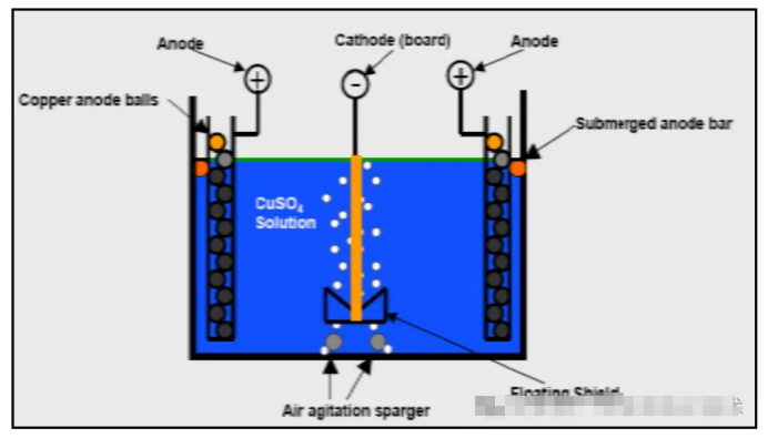
Next, let's introduce the specific principles through the cover image.
Chemical composition and function:
CuSO4: Provides the Cu2+ required for electroplating, helping the transfer of copper ions between the anode and cathode
H2SO4: Enhances the conductivity of the plating solution
Cl: Assists in the formation of the anode film and the dissolution of the anode, helping to improve the deposition and crystallization of copper
Electroplating additives: Improve the fineness of the plating crystallization and the deep plating performance
Chemical reaction comparison:
1. The concentration ratio of copper ions in the copper sulfate plating solution to sulfuric acid and hydrochloric acid directly affects the deep plating capability of through and blind holes.
2. The higher the copper ion content, the poorer the electrical conductivity of the solution, which means the greater the resistance, leading to poor current distribution in one pass. Therefore, for high aspect ratio through-holes, a low copper high acid plating solution system is required.
3. For blind holes, due to the poor circulation of the solution inside the holes, a high concentration of copper ions is needed to support the continuous reaction.
Therefore, products that have both high aspect ratio through-holes and blind holes present two opposite directions for electroplating, which also constitutes the difficulty of the process.
In the next article, we will continue to explore the principles of research on electroplating for HDI PCBs with high aspect ratios.