
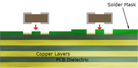
The Layer of Solder Mask on PCB
In general, the solder mask thickness in the middle position of the line is generally not less than 10 microns, and the position on both sides of the line is generally not less than 5 microns, which used to be stipulated in the IPC standard, but now it is not required, and the specific requirements of the customer shall prevail.
As for the thickness of the spray tin, horizontal spray tin thickness is divided into three types: 2.54mm (100mil), 5.08mm (200mil), 7.62mm (300mil).
In the IPC standard, the nickel layer thickness of 2.5 microns or more is sufficient for Class II boards.
Hole requirements to be checked from the degreasing, micro-etching, plating tanks, the main reasons for the impact include: contaminated particles, blower tubes, filter pump leakage, low salt content, high acid content, additives lack of the main wetting agent, there may be a number of metal ions contamination and so on. A class of board is mainly due to the above reasons, as for the clip film, to can be ink or dry film, you can make some improvements from the process, generally may be due to the uneven distribution of some of the board's graphic in the plating is ignored and caused!


