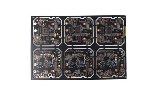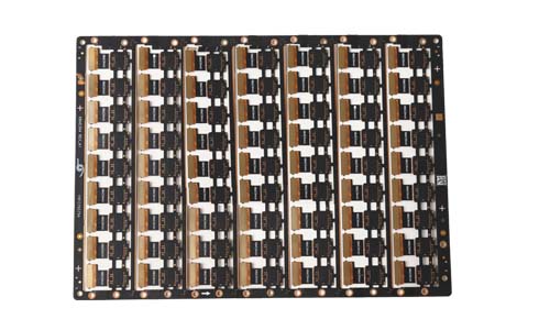
Our 6-layer precision medical equipment PCB circuit board is designed for demanding medical applications, with excellent performance and reliability, meeting the strict requirements of modern medical equipment for precision, stability and durability.
6-layer Precision Medical Equipment PCB Circuit Board Product Introduction
 |
 |
1.Product Overview
Our 6-layer precision medical equipment PCB circuit board is designed for demanding medical applications, with excellent performance and reliability, meeting the strict requirements of modern medical equipment for precision, stability and durability. The circuit board adopts advanced manufacturing technology and high-quality materials to ensure superior performance in various environments.
2.Main Features
High layer count design:
Adopt 6-layer design to provide higher circuit density and better signal integrity, suitable for complex medical equipment applications.
High-quality materials:
Use high-frequency materials (such as FR-4, PTFE, etc.) with good thermal stability and low loss characteristics to ensure the reliability of signal transmission.
Precision manufacturing process:
Adopt high-definition lithography and laser cutting technology to ensure fine lines and small spacing, adapting to the layout of high-density components.
Multiple surface treatment options:
Provide a variety of surface treatment methods, such as HASL, ENIG, OSP, etc., to meet the needs of different customers and ensure welding performance and corrosion resistance.
Excellent thermal management:
The design takes thermal management into consideration, and through reasonable laminated structure and thermal conductive materials, the stability of the equipment during long-term operation is ensured.
Compliance with medical standards:
The product complies with medical industry standards such as ISO13485 and IEC60601 to ensure the safety and reliability of the product.
3.Application areas
Monitoring equipment: such as ECG monitors, vital signs monitors, etc.
Imaging equipment: such as ultrasound equipment, X-ray machines, CT scanners, etc.
Therapeutic equipment: such as laser therapy equipment, physical therapy equipment, etc.
Laboratory equipment: such as analytical instruments, diagnostic equipment, etc.
4.Technical Specifications
| Number of layers | 6 | Minimum line width / line spacing | 0.1mm / 0.1mm |
| Board thickness | 1.6mm (customizable) | Impedance control | ±10% |
| Copper thickness | 1oz / 2oz (customizable) | Test standard | Each board is 100% electrically tested |
5. Advantages of Nickel-palladium-gold Process
The advantages of nickel-palladium-gold process include stable durability, excellent solder resistance, good compatibility, high plating flatness, suitable for high-density pads, and relatively low cost. In addition, the process has the following advantages:
Prevent the occurrence of "black nickel problem": separate nickel and gold through the palladium layer to prevent nickel and gold displacement migration.
The chemically plated palladium layer acts as a barrier layer, and there will be no problem of copper migrating to the gold layer, resulting in poor solderability.
The chemically plated palladium layer is completely dissolved in the solder, and no high-phosphorus layer will appear on the alloy interface.
Can withstand multiple lead-free reflow cycles and has excellent gold wire bonding.
Resistant to storage, high solder joint reliability, can be reflowed multiple times.
 |
 |
6.Production Capacity
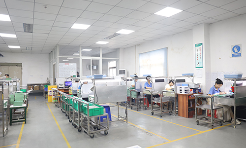
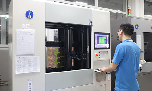
We have advanced production equipment and a professional technical team with large-scale production capabilities to meet the diverse needs of customers. Support small-batch trial production and large-scale production with timely delivery.
7.Customer Support
Provide comprehensive technical support and after-sales service to assist customers in solving various problems during design, manufacturing and post-maintenance.
8.Conclusion
Our 6-layer precision medical device PCB circuit board is an ideal choice for your medical product development. With its high performance, high reliability and compliance with industry standards, it will help your medical device stand out in the market. For more information or to get a quote, please feel free to contact us.
FAQ
Q: How far is your factory from the nearest airport?
A: About 30 kilometers.
Q: What is your minimum order quantity?
A: One piece is enough to place an order.
Q: How to resolve short circuits and open circuits in communication PCBs?
A: Short circuits and open circuits are usually caused by circuit aging or manufacturing defects, and need to be resolved through careful inspection and professional repair methods.
Q: How many layers of HDI can your company produce?
A: We can produce from four layers of first order to high multi-layer arbitrary interconnect PCB circuit boards.