
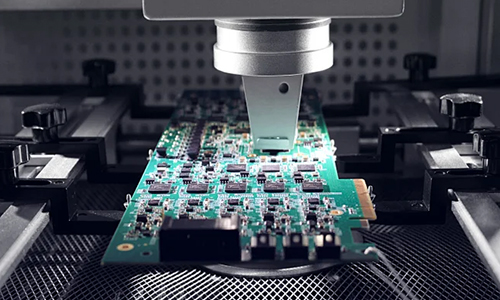
Double-sided medical PCB is a PCB widely used in medical equipment with good electrical performance and reliability.
Technical Parameters
| Number of layers | 2L | Minimum aperture | 0.7mm |
| Board thickness | 1.6mm | Surface treatment | tin spraying |
| Board material | FR-4 SY1141 | Minimum hole copper | 25um |
| Ink color | red oil with white characters | Copper thickness | 35um |
| Minimum line width/distance | 0.33mm/0.17mm | / | / |
| WHY US |
||||
 |
 |
 |
||
| Fast Delivery | High Quality | Diversified Customization | ||
| Factory | ||||
 |
 |
 |
||
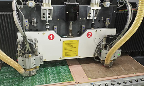
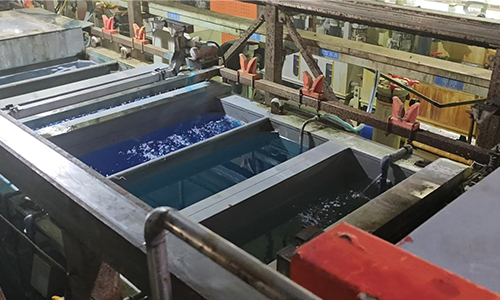
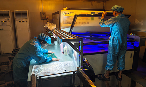
| Photoengraving Workshop | Drilling Machine | Electroplating Production Line | ||
| More Information | ||
| Strategic Partners | Application | Certificate |
FAQ
1.Q: When can I get a quotation after I provide Gerber, product process requirements?
A: Our sales staff will give you a quotation within 1 hour.
2.Q: How many employees do you have in your factory?
A: More than 500.
3.Q: What is the primary role of the palladium layer in nickel palladium gold PCBs?
A: It prevents the migration of copper from the copper layer to the gold layer, which can lead to poor solderability.
4.Q: Can a lack of strict control during the production process lead to many problems?
A: In the production process, issues such as uneven plating thickness and inaccurate milling can negatively impact the performance of PCB. Therefore, strict control of the production process is key to ensuring quality.