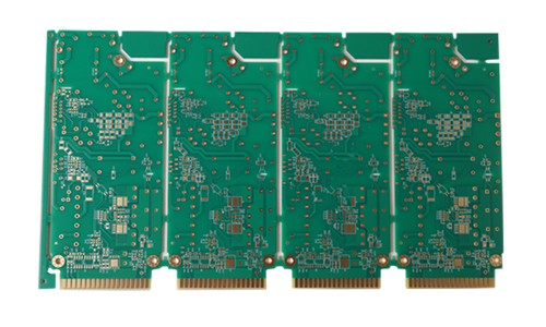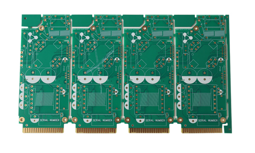
Four-layer gold finger board module PCB board is a printed circuit board designed for connection and signal transmission, which is widely used in various electronic devices, such as computers, communication equipment and consumer electronics.
Four-layer Gold Finger Board Module PCB Board Product Introduction
 |
 |
1.Product Overview
Four-layer gold finger board module PCB board is a printed circuit board designed for connection and signal transmission, which is widely used in various electronic devices, such as computers, communication equipment and consumer electronics. Gold Finger refers to a metallization treatment on the edge of the circuit board, which is used to provide reliable electrical connection and ensure stable signal transmission.
2.Main Features
Four-layer design:
Adopt four-layer PCB structure to provide good signal integrity and power management.
Through reasonable stacking design, signal interference and crosstalk are effectively reduced.
Gold finger technology:
Adopt gold finger treatment on the edge of PCB to provide excellent conductivity and wear resistance.
Ensure reliable connection with slots or connectors, suitable for application scenarios with frequent plugging and unplugging.
High reliability:
Adopt high-quality materials and advanced manufacturing processes to ensure the stability of PCB in various environments.
Have good moisture resistance, shock resistance and chemical corrosion resistance.
Excellent electrical performance:
Design supports high-speed signal transmission, suitable for data communication and video signal transmission.
Use proper impedance control and differential signal design to ensure signal integrity.
Multiple surface treatments:
Provide multiple surface treatment options such as ENIG, HASL, OSP, etc. to meet different customer needs.
Adapt to different welding processes and environmental requirements.
3.Technical Specifications
| Number of layers | 4 layers | Ink color | green oil white text |
| Material | FR-4, S1000 | Minimum line width/line spacing | 0.1mm/0.1mm |
| Thickness | 1.6mm | Gold finger thickness | 30 wheat |
| Copper thickness | inner 0.5 outer layer 1OZ | Surface treatment | immersion gold |
4.Application Areas
Computer: for motherboards, expansion cards and other computer components.
Communication equipment: for routers, switches and other network equipment.
Consumer electronics: used in smartphones, tablets and other electronic products.
Industrial equipment: used in various industrial control and automation equipment.
 |
 |
5.Conclusion
The four-layer gold finger board module PCB board is a high-performance and reliable product designed to meet the needs of modern electronic devices for connection and signal transmission. Its advanced gold finger technology and excellent electrical performance make it an ideal choice for various applications, providing stable support and efficient connection for electronic devices.
FAQ
Q: What files are used in PCB production?
A: PCB production requires Gerber files and PCB manufacturing specifications, such as the required substrate material, finished thickness, copper layer thickness, solder mask color, and design layout requirements.
Q: When can I get a quotation after I provide Gerber, product process requirements?
A: Our sales staff will give you a quotation within 1 hour.
Q: Can poor solder paste printing occur during the pick-and-place process for gold finger PCB?
A: Yes, if solder paste printing is poor and the printing is repeatedly executed, it may lead to printing quality issues without the need for cleaning. To solve this problem, cleanliness during the printing process should be ensured to avoid quality issues caused by repeated printing.
Q: How thick can your thickest copper be?
A: We could make 10 OZ copper foil.