It is widely used in LED lighting, power amplifiers, lasers, and other high-temperature electronic devices.
Aluminium Nitride Ceramic PCB Product Introduction

1.Product Overview
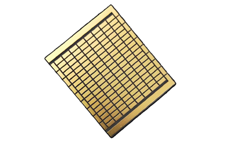
The two-layer aluminum nitride ceramic PCB board is a high-performance printed circuit board that uses aluminum nitride (AlN) as the substrate. Aluminum nitride has excellent thermal conductivity and electrical insulation, which makes this PCB board perform well in high-power and high-frequency applications. It is widely used in LED lighting, power amplifiers, lasers, and other high-temperature electronic devices.
2.Main Features
Excellent thermal conductivity:
The thermal conductivity of aluminum nitride is as high as 170-200 W/m·K, which can effectively dissipate heat, reduce component temperature, and improve overall performance.
High electrical insulation:
It has excellent electrical insulation properties, ensuring the stability and safety of the circuit, and is suitable for high-voltage applications.
High temperature resistance:
It can work for a long time in a high temperature environment, usually withstanding temperatures exceeding 150°C, and is suitable for harsh working conditions.
Good mechanical strength:
Aluminum nitride material has high impact and pressure resistance, ensuring the reliability of the substrate in various application scenarios.
Low dielectric constant and low loss:
Suitable for high-frequency signal transmission, reducing signal attenuation and improving signal integrity.
3.Technical Parameters:
| Number of layers | 2L | Surface treatment | nickel palladium gold |
| Material | Aluminum nitride ceramic | Cutting method | water jet cutting, back covered with blue film |
| Substrate thickness | 0.38mm | Metal single/double-sided | double-sided |
| Metal layer thickness | 350μm | Conduction hole | None |
| Minimum line width | 0.35/0.05mm | Special requirements | urface roughness ≤0.5um |
4.Structure
Two-layer aluminum nitride ceramic PCB board usually consists of the following two layers:
First layer: signal layer, responsible for transmitting electrical signals, usually connected by metallized hole technology.
Second layer: bottom layer, providing mechanical support and protection, and can also be used as a ground layer to enhance the anti-interference ability of the circuit.
5.Application Areas
LED lighting: used for heat dissipation and drive circuits of high-power LEDs.
Power amplifier: provides good thermal management in communication and RF applications.
Laser: Circuit boards for laser transmitters to ensure stability and reliability.
Automotive electronics: such as control systems and sensors for electric vehicles.
 |
 |
6.Conclusion
Double-layer aluminum nitride ceramic PCB boards have become indispensable materials in high-power and high-frequency electronic devices due to their excellent thermal management and electrical performance. With the continuous advancement of technology, its application areas will continue to expand, providing more efficient and reliable solutions for various industries.
FAQ
Q: Do you have an office address that could be visited?
A: Our office address is Tianyue Building, Bao 'an District, Shenzhen.
Q: Will you attend the exhibition to show your products?
A: We are planning on it.
Q: How many specific materials are there for ceramic PCB boards?
A: There are four main core materials for ceramic PCB boards: alumina, aluminum nitride, silicon nitride, and gallium nitride. These materials are used to fabricate alumina ceramic PCB, aluminum nitride ceramic PCB, silicon nitride ceramic PCB, and gallium nitride ceramic PCB, respectively. Each of these materials is an insulating and thermally conductive material with slightly different applications. Aluminum nitride ceramic PCB have the highest thermal conductivity, while silicon nitride ceramic PCB offer better mechanical strength.
Q: What is the difference between ceramic circuit boards and traditional PCB? Can ceramic substrates replace PCB boards?
A: Ceramic circuit boards, also known as ceramic PCB or ceramic substrates, are distinguished by their superior heat dissipation properties compared to traditional PCB. Traditional PCB typically have a thermal conductivity of 1W to 3W, whereas ceramic PCB can range from 15W to 170W, which is ten to hundreds of times greater than that of traditional PCB. Although ceramic substrates are excellent, they may not replace all PCB. In applications requiring thermal conduction but not extensive heat dissipation, ceramic substrates are likely to be used. However, in many fields where traditional PCB do not demand high product specifications, using PCB can reduce costs. After all, the price and production process of FR4 and ceramic substrate materials are not comparable.
Q: What is the use of ceramic PCB? Where are ceramic PCB used?
A:ceramic PCB have a wide range of applications. They are used in high-power power electronic modules, solar panel components, high-frequency switching power supplies, solid-state relays, automotive electronics, aerospace, military electronic products, high-power LED lighting products, communication antennas, automotive ignition systems, insulation resistance ceramic PCB, semiconductor devices, and refrigeration equipment, among others.
Q: How long does it generally take to deliver HDI high-frequency PCB?
A: We have raw material inventory (such as RO4350B, RO4003C, etc.), and our fastest delivery time can be 3-5 days.