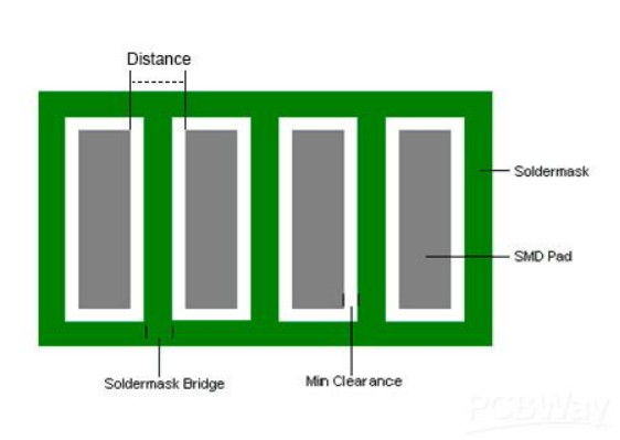

Following up on the last news, this news article continues to learn the acceptance criteria for the quality of PCB solder mask process.
Line Surface Requirements:
1.No oxidation of the copper layer or fingerprints are allowed under the ink.
2.The following conditions under the ink are not acceptable:
① Debris under the ink with a diameter greater than 0.25mm.
② Debris under the ink that reduces the line spacing by 50%.
③ More than 3 points of debris under the ink per side.
④ Conductive debris under the ink that spans across two conductors.
3. No redness of the lines is allowed.
BGA Area Requirements:
1.No ink is allowed on the BGA pads.
2.No debris or contaminants that affect solderability are allowed on the BGA pads.
3.Holes in the BGA area must be plugged, with no light seepage or ink overflow. The height of the plugged via should not exceed the level of the BGA pads. The mouth of the plugged via should not exhibit redness.
4.Holes with a finished hole diameter of 0.8mm or greater in the BGA area (ventilation holes) do not need to be plugged, but exposed copper at the hole mouth is not allowed.