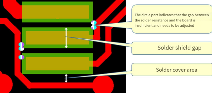

Today we will learn that, in the PCB solder mask, specifically should be in accordance with which standards to process. The following acceptance criteria apply to PCB in the solder mask process or after processing, product production process monitoring and product quality monitoring.
Alignment Requirements:
1. Upper Pads: The solder mask on the component holes should ensure that the minimum solderable ring is not less than 0.05mm; the solder mask on the via holes should not exceed half of the solder ring on one side; the solder mask on the SMT pads should not exceed one-fifth of the total pad area.
2. No Exposed Traces: There should be no exposed copper at the junction of the pad and the trace due to misalignment.
Hole Requirements:
1. Component holes must not have any ink inside.
2. The number of via holes filled with ink must not exceed 5% of the total via hole count (when design ensures this condition).
3. Through holes with a finished hole diameter of 0.7mm or greater that require solder mask coverage must not have ink plugging the holes.
4. For via holes that require plugging, there must be no plugging defects (such as seeing light through) or ink overflow phenomena.
More acceptance criteria will show in the next news.