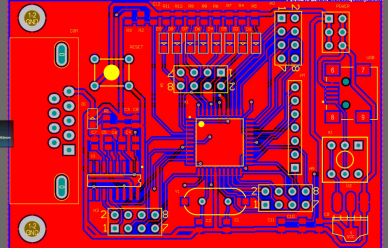

During our regular PCB design, we encounter various safety clearance issues, such as the spacing between vias and pads, and the spacing between traces, which are all aspects we should consider. Today, we will categorize these clearance requirements into two types: one is electrical safety clearance; the other is non-electrical safety clearance. Let's start with the electrical safety clearance:
Electrical Safety Clearance:
Trace to Trace Spacing:
According to industry regulations, the spacing between traces must not be less than 4 MILS. The term "trace to trace" also refers to the spacing from trace to pad. From a production standpoint, the larger the spacing, the better, under the condition that it is possible. A conventional standard is generally 10 MILS.
Pad Hole Diameter and Pad Width:
When drilling holes in the PCB process, if the pad hole diameter is drilled mechanically, it must not be less than 0.2mm. If laser drilling is used, it must not be less than 4 MILS. The tolerance of the hole diameter varies slightly depending on the material. Generally, the error can be controlled within 0.05mm. The pad width must not be less than 0.2mm.
In the next article, we will introduce the other two electrical safety clearances: the safe clearance between pads and the safe clearance between copper foil and the board edge.