
Today let’s continue to the next tip in PCB routing:
In the context of PCB manufacturing, adding a common ground plane beneath signal traces is a standard practice. The purpose of this design is to ensure that the impedance between any two ground points on the PCB is minimized, thereby reducing interference and signal loss during transmission. The ground plane provides a stable reference plane that helps maintain signal integrity, especially important in high-speed signal transmission.
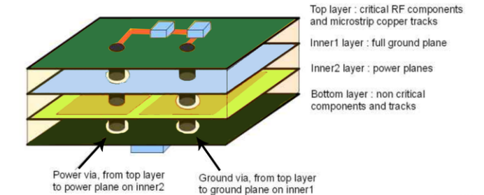
When the outer layer adjacent to the ground plane is used for mounting high-speed components, such as RF components using microstrip or coplanar lines, the other side can be used for less critical components. The second inner layer is typically used for a power plane, which should be as large as possible to reduce impedance. This provides a low impedance power path, helping to reduce power noise and improve power stability.
To reduce costs, double-sided PCBs can be used with ground planes added on both sides of the interconnected traces through numerous vias. This design can provide good signal and power integrity without significantly increasing costs.
Setting isolated ground planes for single-point interconnected logic and analog components can reduce ground plane noise. This means that if signals from one area need to be isolated from those of another, independent ground planes can be set between them. Additionally, traces connecting one area to another should be arranged above the interconnection points to minimize interference during signal transmission and improve signal quality.
In summary, these design principles and techniques are aimed at improving signal integrity and power integrity on the PCB, ensuring the stable and reliable operation of electronic devices. By careful layout and design, high-performance PCB designs can be achieved without significantly increasing costs.


