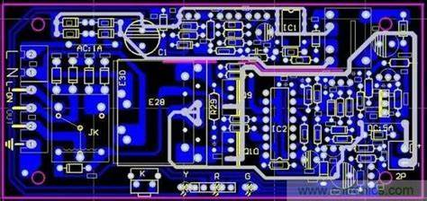

Now let’s learn about another 3 common rules: 3W/4W/10W Rule, Overlap of Power and Ground Planes Rule, and 1/4 Wavelength Rule.
1. 3W/4W/10W Rule (W: Width):
The 3W/4W rule is primarily aimed at suppressing electromagnetic radiation and preventing crosstalk between closely placed traces.
In PCB design, the distance between traces should follow the 3W rule, which means maintaining a distance of three times the trace width between lines. This can maintain 70% of the electric field from interfering with each other. For differential pairs, the gap spacing should meet the 4W rule.
To achieve 98% non-interference of the electric field, the 10W rule can be applied.
During the design process, if it is not possible to meet the 3W rule for all signal lines, sensitive signals such as clock signals and reset signals can be treated with the 3W rule.
2. Overlap of Power and Ground Planes Rule
Different power planes should avoid overlapping in space to reduce interference between different power sources, especially those with significantly different voltages.
The overlap of power planes should be avoided if possible, and if unavoidable, a ground plane can be inserted in between.
3. 1/4 Wavelength Rule
The 1/4 wavelength rule states that the length of a PCB trace should be less than 1/4 of the wavelength of the signal on that trace.
A trace that is 1/4 of a wavelength long acts as an excellent radiating antenna. The wavelength (λ) is calculated as the speed of light divided by the frequency. It is generally recommended that the trace length be less than 1/20λ for optimal performance.
For example, for a 100MHz signal, the wavelength is 3 meters, 1/4λ is 75cm, and the trace length should not exceed 1/20λ, which is 15cm.