
Let's continue to learn about the rest of 4 situations and methods to reduce the tight delay deviation.
1. To reduce the tight delay deviation, if signal speed matching is required, it is best to route all traces within the same interface on the same layer, reducing uncertainties and potential signal delays due to inter-layer transmission, as shown in the cover figure.
2. In PCB design, the length of internal routing within capacitor pads is also a factor to consider. Even if the signal does not directly pass through these internal traces, some CAD (Computer-Aided Design) tools will include these trace lengths in their calculations and display the length difference between positive and negative signals. To minimize this situation, ensure that the pad entries for both signals are equal in length to reduce signal length discrepancies caused by improper pad design.

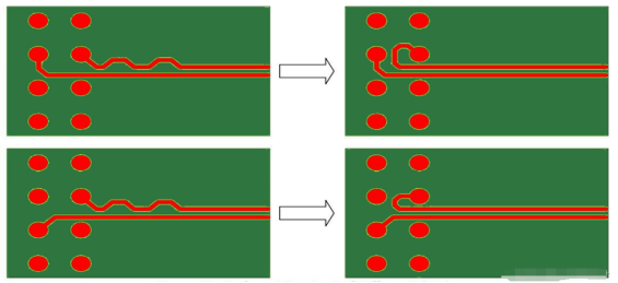
3. In the design of differential pair signals, asymmetrical branching is a preferred method as it can reduce signal interference. When routing, serpentine routing should be avoided whenever possible, as it may increase signal propagation delay and impedance discontinuities, affecting signal integrity, as shown in the figure below.

4. If there is enough space between pads, consider including small loops for shorter traces instead of using serpentine routing. Vias, which are conductive holes connecting different layers, are generally preferred over serpentine routing because they provide a shorter, more direct connection path, reducing signal delay, as shown in the figure below.

The above points outline the 8 key considerations for serpentine routing in PCB design, which are crucial for ensuring circuit performance and signal integrity.