
Let’s continue to learn about the various types of holes found on HDI PCB.
1. Tangency hole
Tangent holes refer to holes that are part of the same network, where laser holes and other laser holes or structural holes are intentionally offset from each other.
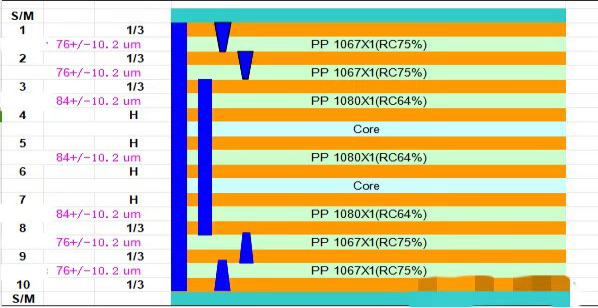
The PCB stackup is shown in the cover picture above. This way, the cost of achieving a second-order connection is lower. The holes of the same network can only be tangent to the outer pads, and cannot intersect. This type is known as a pseudo second-order hole. The stackup in the next picture is also known as a 10-layer pseudo second-order board, with the mathematical expression being "1+1+6+1+1".
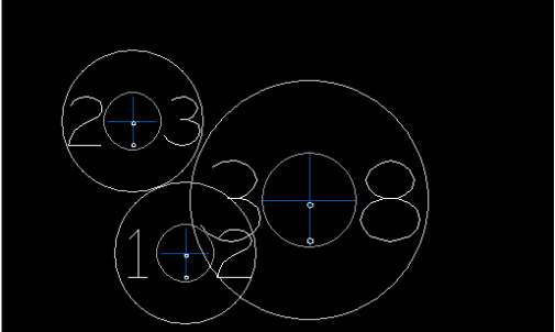
As shown in the figure below, all three holes have the GND attribute, with holes 1-2 and 2-3 being tangent, and holes 2-3 and 2-8 also being tangent, thus maintaining the closest possible distance between them. This configuration is used to optimize the routing of signals and to reduce electromagnetic interference within the PCB.
2. Superimposed hole
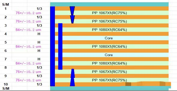
Stacked holes are holes where laser holes or structural holes within the same network overlap each other. As shown in the figure below, holes 1-2 and 2-3 of the same network coincide, forming a single 1-3 hole, and holes 8-9 and 9-10 coincide, forming a single 8-10 hole. This type of layering is known as a 10-layer second-order stacked hole board, also called a 10-layer true second-order board, with the mathematical expression being "2+6+2".
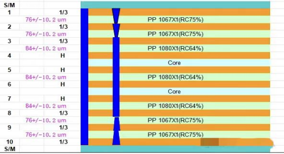
Of course, it is also possible to create a stacked hole with both laser and mechanical holes, as shown in the following layered structure. Four laser holes of the same network and one mechanical hole are superimposed to form a through-hole with different hole diameters. This is the ultimate level of stacked holes and represents the highest level of craftsmanship in stacked hole production. However, the cost of this processing is too high, and few design companies adopt this kind of layering for design.
More kinds of holes will be shown in the next new.


