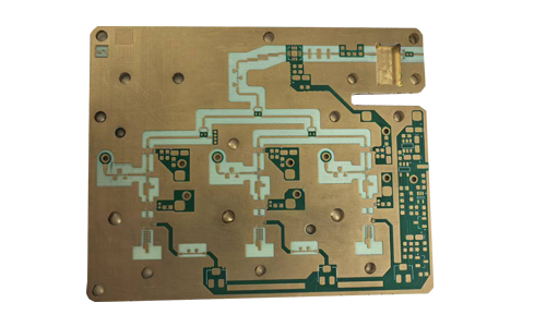
Double-sided Thermoelectric Separation Copper Substrate is a high-performance PCB designed to meet the requirements of high-power electronic devices and thermal management.
Metal PCB Copper Based Board Product Introduction

1.Product Overview
Double-sided Thermoelectric Separation Copper Substrate is a high-performance PCB designed to meet the requirements of high-power electronic devices and thermal management. The substrate uses copper as the conductive substrate and combines thermoelectric separation technology to effectively reduce heat accumulation during device operation and improve overall performance and reliability. Such substrates are widely used in LED lighting, power amplifiers, automotive electronics, industrial control and other fields.
2.Product Features
1.Excellent thermal management:
2.Copper material has excellent thermal conductivity, which can quickly dissipate heat, effectively reduce heat accumulation, and ensure that electronic components operate at the optimal operating temperature.
3.Double-sided design:
4.Double-sided layout provides greater design flexibility, supports the integration of multi-layer circuits, and adapts to complex circuit requirements and compact space constraints.
5.Thermoelectric separation technology:
6.Thermoelectric separation technology can effectively isolate heat sources from sensitive electronic components, reduce the impact of heat on circuit performance, and improve system stability and reliability.
7.High reliability:
8.The substrate has undergone strict quality control and environmental testing to ensure its reliability in harsh environments such as high temperature, high humidity and vibration, and is suitable for applications with long-term operation.
9.Strong compatibility:
10.Supports a variety of components and packaging forms, suitable for different electronic design and manufacturing needs.
11.Excellent electrical performance:
12.Use high-quality insulating materials to ensure good electrical insulation performance and signal integrity, and reduce electromagnetic interference (EMI).
3.Technical Specifications
| Number of layers | 2 layers | Ink color | green oil and white text |
| Material | copper | Minimum line width/line spacing | 0.3mm/0.3mm |
| Thickness | 2.0mm | Is there solder mask | no |
| Copper thickness | 1OZ | Surface treatment | immersion gold |
4.Application Areas
LED lighting: widely used in high-power LED lighting equipment, providing good heat dissipation solutions.
Power amplifier: In the field of wireless communication and broadcasting, as a substrate for power amplifiers, it ensures high efficiency and reliability.
Automotive electronics: used in automotive power management and thermal management systems to improve the performance of electronic equipment.
Industrial control: In industrial automation equipment, as the basis of control circuits, ensure high efficiency and stability.
5.Production Process
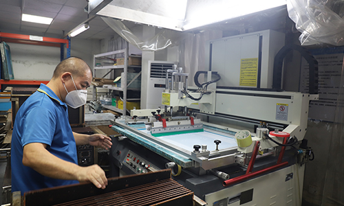
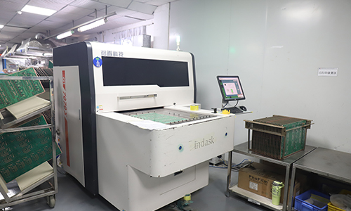
Precision etching and laser drilling: Ensure the accuracy of circuit patterns to meet the design requirements of high-density interconnection (HDI).
Multilayer lamination technology: Use high temperature and high pressure processes to combine different layers of materials to ensure electrical performance and mechanical strength.
Surface treatment: Provide a variety of surface treatment options, such as electroless gold plating (ENIG), hot air leveling (HASL), etc. to improve welding reliability and corrosion resistance.
 |
 |
6.Conclusion
Double-sided thermal and electrical separation copper substrate has become an indispensable and important part of modern high-power electronic devices with its excellent thermal management performance and reliability. It can not only effectively reduce the impact of heat on the circuit, but also improve the overall performance and service life of the equipment, and is suitable for various high-demand electronic applications. As the requirements for heat dissipation performance of electronic equipment continue to increase, this substrate will play an increasingly important role in future electronic design.
FAQ
Q: How far is your factory from the nearest airport?
A: About 30 kilometers.
Q: What is your minimum order quantity?
A: One piece is enough to place an order.
Q: What are the key factors to consider when designing an IC carrier PCB?
A: When designing an IC carrier PCB, the following key factors should be considered:
1) Signal Integrity: IC carrier boards need to transmit a large number of signals, and the design should ensure the integrity of the signals, reducing signal interference and loss.
2) Electromagnetic Compatibility: The design should consider electromagnetic compatibility to reduce interference between different signals.
3) High-Speed Signal Transmission: For signals requiring high-speed transmission, the design should consider the stability and reliability of signal transmission, reducing signal delay and distortion.
Q: Can your company manufacture impedance boards and crimp hole circuit boards?
A: We can produce impedance PCB, and the same product can be made with multiple impedance values. We can also manufacture precision holes for crimp holes.